Adjustable stiffness center via 6 DoF maglev
Step and flash imprint lithography (SFIL) is a process that is used for pattern replication of thin layers on a substrate material for creating details with sub-100 nm dimensions with high aspect ratio [1]. After a photopolymerization-replication step with a low viscosity organosilicon solution, pattern transfer is realized through wet or dry etching into a layer on the substrate (wafer). To assure a uniform etch barrier layer thickness, typically, flexure-based mechanisms are used in the wafer chuck or template holder to allow for relative alignment in the order of 1 µrad [2].
Description
Accurate template-to-wafer alignment is key in SFIL processes, both during contacting of the template to the transfer layer on the wafer, but also during template separation to avoid lateral shear motion in the high aspect ratio features. In the SFIL machine architectures developed from the late 1990s, so-called (passive) flexure mechanisms were used, both in the wafer support (Figure 1) and the template holder (Figure 2) to compensate for geometry errors from machining, machine assembling, and positioning uncertainty involved in wafer and template loading/unloading [1,2].
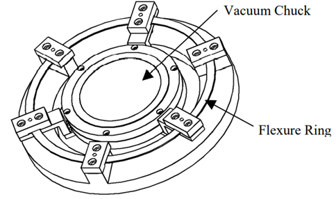  | 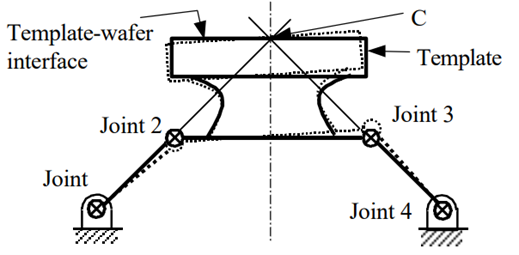  |
| Figure 1. Flexure mechanism for wafer vacuum chuck based on an aluminum flexure ring with 3-fold symmetry [1]. | Figure 2. Flexure mechanism for template holder based on four bar linkage with virtual point of rotation at the template-to-wafer interface (C), allowing for the use multiple templates in parallel [2]. |
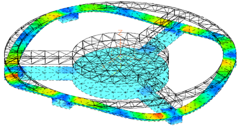
In addition, as a result of distributed structural compliances in the system, the imprint or release forces of up to 100 N may result in additional displacements (rotations and translations) and deformations that negatively affect the imprint performance (see Figure 3). In view of these large process forces in SFIL (as opposed to optical lithography), passive bearing systems, such as air bearings and roller bearings, as well as template holders may give additional quasi-static deformations and (parasitic) lateral motion from resulting misalignment (tip and tilt) between template and wafer. Particularly for high resolution nano imprint, it may be beneficial to provide a local center of stiffness at the die of interest. The center of stiffness of a structure can be defined as the point, through which the sum of external forces result in pure translations without parasitic rotational effects.
 |  |
| Figure 3. Schematic representation of SFIL system that is affected by distributed structural compliances in the wafer stage. | Figure 4. Schematic representation of maglev stage concept, which allows for creating a center of stiffness at the (subsequent) die of interest and compensation of quasi-static deformations such as tip and tilt motion of stage and template and in-plane displacement during the imprint process [3]. |
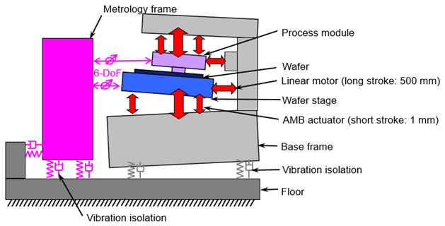
Therefore, as an alternative for passive bearing systems as well as for flexure mechanisms in the wafer chuck or template holder (that goes with a stiffness penalty in axial direction), active magnetic bearing (AMB) or magnetic levitation (maglev) systems can be used. These active systems can compensate for quasi-static deformations and (parasitic) lateral motion during imprint and release.
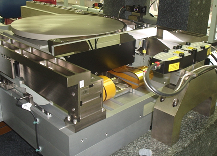 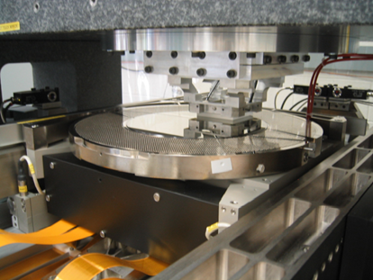 |
| Figure 5. Prototype maglev stage for 300 mm semiconductor application with full 6-DoF motion capability and 6 DoF isolation (left), and stage in combination with SFIL template (right). |
By controlling the stage 6-axis position based on metrology as close as possible to the substrate and template (Abbe principle), a (theoretically) infinite static stiffness can be obtained, and a 6-DoF active stiffness center created at the subsequent die of interest [3]. Dynamic stiffness obviously is limited, first and foremost by the bandwidth of the feedback control system, but can be favorably high by designing for high internal resonance frequencies. In addition to enabling a center of stiffness, maglev stages allow for ultra-low contamination and a full 6-DoF isolation from the supporting machine base, resulting in greatly reduced sensitivity for disturbances e.g. from previous setpoints or fab floors, roughly by a factor 103 to 104 compared to stages with conventional passive bearing systems [4].
Figure 5 shows a prototype of a 300 mm maglev stage that was designed for SFIL application [3]. The stage is based on variable reluctance actuators for the high efficiency (see Figure 6). Since the actuators operate at relatively large gap in the order of ±1 mm, tip/tilt correction for wafer leveling purposes, as well as wafer alignment capabilities are inherently present without the necessity of stacking additional stages on top. Off-line actuator calibration is required for the inherent actuator non-linearity of the force depending on both current and gap squared (see also [5]). Here, the stage 6-DoF position information is used for magnetic gap reconstruction as shown in Figure 6.
 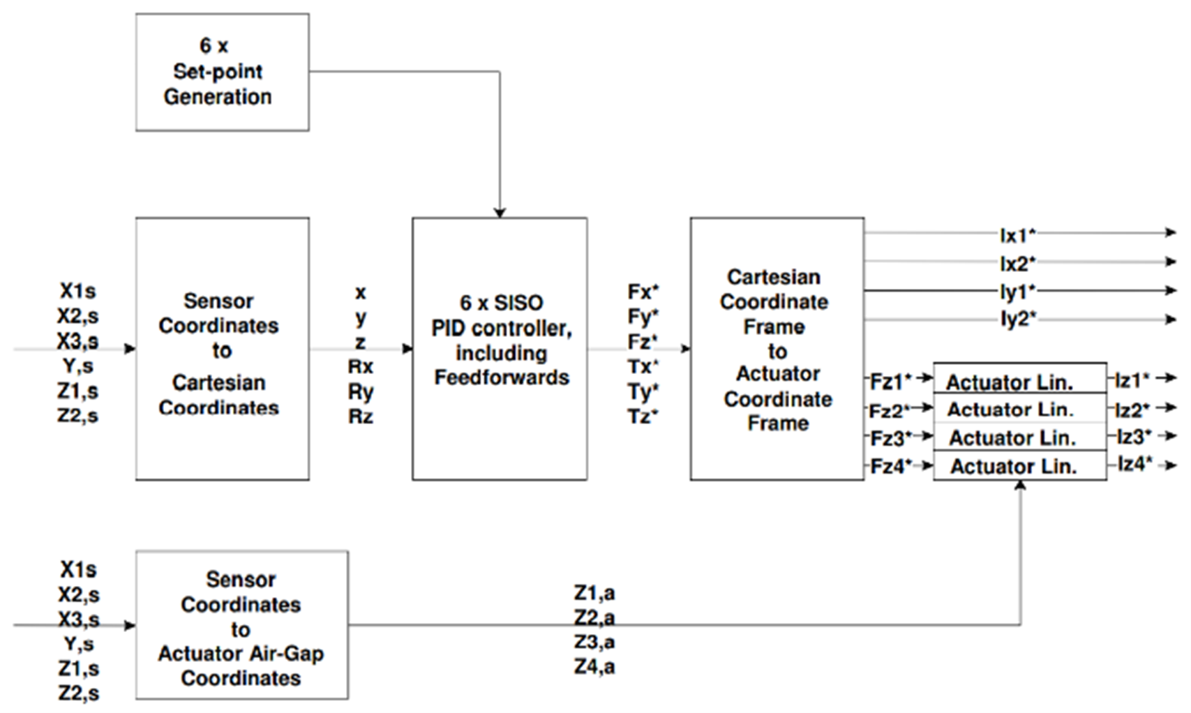 |
| Figure 6. Maglev actuator concept and force vs. current for different actuator magnetic gaps (left), and 6 DoF motion control scheme including gap reconstruction and actuator linearization (right) [3]. |
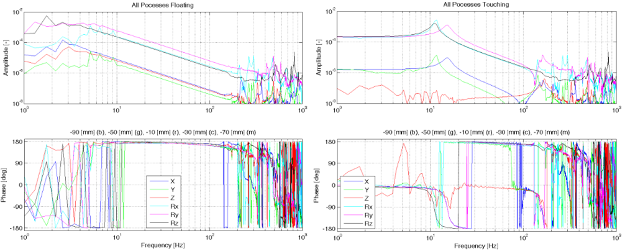 |   |
| Figure 8. Frequency response functions (FRFs) of the free floating stage (left) and the stage in contact with the template (right). | Figure 9. Auto leveling and stable imprinting of edge dies. |
Controller switching is required upon wafer-to-template contact and release in view of changing system dynamics to guarantee stability. FRFs of the free-floating stage and the stage during imprint in contact with the template are shown in Figure 7. In experiments, the following key features of the maglev architecture for use in SFIL were demonstrated:
- Auto-leveling capability of wafer-to-template: Sub µrad accuracy and repeatability obtained within 0.5-1 sec.
- Stable imprint capability of edge dies: Stiffness center programmable to coincide with the center of gravity of the die of interest, also for partial (edge) dies, which enhances yield (see Figure 8).
- Stable template release after the imprint process: Fully controlled release perpendicular to the template surface based on separation detection and controller switching.
| Application: Step and flash imprint lithography for sub-100 nm features. | Realized: Prototype planar maglev stage. | Principle: Adjustable stiffness center via 6 DoF maglev technology. |
References
[1] Colburn, M., Johnson, S., Stewart, M., Damle, S., Bailey, T., Choi, B., Wedlake, M., Michaelson, T., Sreenivasan, S.V., Ekerdt, J., Willson, C.G., Step and flash imprint lithography: A new approach to high-resolution patterning, Proc. of SPIE 3676(I), 1999.
[2] Choi, B.J., Johnson, S., Sreenivasan, S.V., Colburn, M., Bailey, T., Willson, C.G., Partially constrained compliant stages for high resolution imprint lithography, Proc. of 2000 ASME Design Engineering Technical Conference, Baltimore, MD, September 10-13, 2000.
[3] Vermeulen, J.P.M., Peijnenburg, A.T.A., Norg, M.L., Musall, T.W., Eijk, J. van, Active magnetic bearing technology suitable for nanoimprint lithography applications, Proc. of the International Conference on Nanoimprint and Nanoprint Technologies 2006 Conference, San Francisco, CA, November 15-17, 2006.
[4] Peijnenburg, A.T.A., Vermeulen, J.P.M., Eijk, J. van, Magnetic levitation systems compared to conventional bearing systems, Proc. of the 31st International Conference on Micro- and Nano-Engineering, Vienna, Austria, pp. 1372-1375, 2005.
[5] Klerk, A.C.P., Angelis, G.Z., Design of a magnetically levitated 6 DoF stage for scanning applications, Proc. of ISMST8, 2005.
Development
Meindert Norg, Hans Vermeulen, Ton Peijnenburg, Philips Apptech (2005)